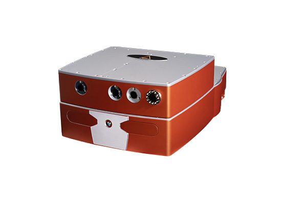
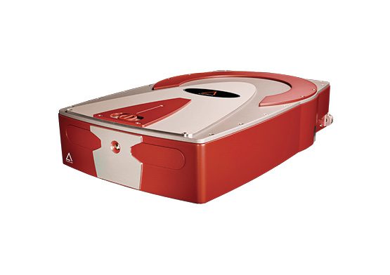
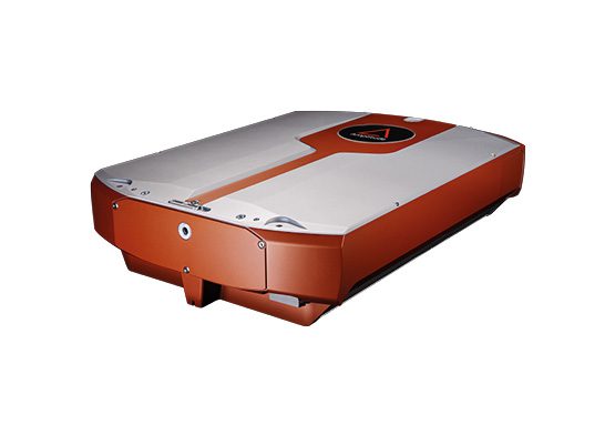
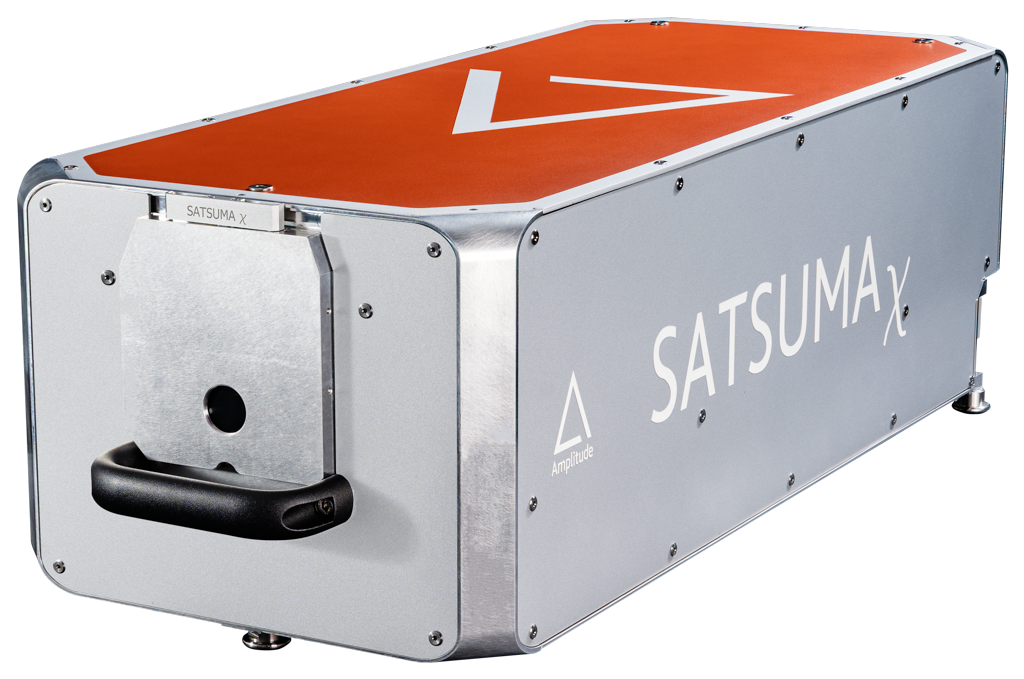
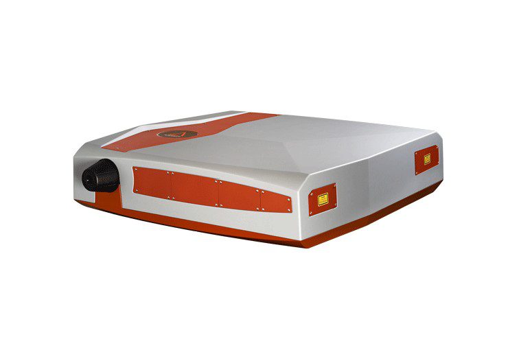
The display panel industry has witnessed a rapid and remarkable evolution over the past decades, transitioning from LCD to OLED panels and now to cutting-edge µLED and OLED technology. This constant innovation in display imposes continuous challenges in manufacturing processes. With demands for novel features, freeform shapes, the use of new materials, and the pursuit of high-definition displays across a large spectrum of devices, including smartphones, IT products (tablets, laptops, monitors), TV, and now VR/AR products, this industry is in need of advanced solutions. These solutions must deliver the utmost precision, quality, and productivity.
Femtosecond laser technology is an excellent alternative to more traditional laser technologies and is often the only available solution on the market.
Advantages of Laser Technology in Flat Panel Displays
The adoption of laser technology in flat panel display manufacturing brings forth a multitude of benefits:
- Unmatched Precision: Femtosecond lasers allow tight focusing with excellent beam quality, enabling microscopic precision for accurate cutting, drilling, and selective ablation.
- High Quality: Femtosecond laser/matter interaction allows an ablation with limited thermal effects (Heat Affected Zone – HAZ). As a result, cutting, drilling, or selective ablation processes are performed with unrivalled quality.
- Excellent Productivity: Femtosecond lasers are now capable of reaching high power levels, which enables high-speed processing.
What can we do with Ultrashort Pulse lasers in Display manufacturing?
OLED Repair

Array Repair
Display panels are made of a TFT (Thin Film Transistor) array. This TFT array is made of multiple thin film layers of various types of materials. During the manufacturing process, the arrays of pixels are often exposed to possible contamination (dust) or defects. Thanks to femtosecond lasers, we can now fix such abnormalities furing manufacturing, to optimize the quality of the display, thus boosting production yield.
Cell Repair
Other than Array repair, a new application has emerged over the past few years – Cell Repair. The cell process comes later in the manufacturing chain, where contamination and defects can also occur. Femtosecond lasers can address such issues, increasing the production yield for panel makers.
OLED Cutting
Over the past years, one of the main trends in display production has been to improve the “Display Area” ratio vs. “Device Area.” Consequently, features like “Bezel-less,” “Notch,” “HIAA” (Hole in Active Area), and “UPC” (Under Panel Camera) have been developed to achieve this goal. Femtosecond lasers are one of the major tools that has allowed such features to exist.
Today, femtosecond lasers are used for the two following groups of cutting applications:
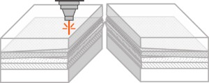
Shape Cutting
High-power UV femtosecond lasers are used in mass production to perform such cuts. Thanks to its unique cutting precision, excellent cutting quality, and high productivity, the high-power UV femtosecond laser has replaced the high-power UV picosecond laser in the field.
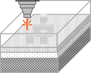
Hole Cutting
Making a hole in the active part of an OLED panel intrinsically requires high precision and a limited affected zone. Again, UV femtosecond lasers are an ideal tool for all related applications.
