The semiconductor industry has been a driving force behind the evolution of technology with increasingly powerful capabilities. Laser technology has become a vital tool in changing how semiconductors are manufactured, from wafer slicing to the device’s packaging; numerous laser technologies are now the standard tool to perform lithography, inspection, thickness metrology, wafer dicing, high-density drilling, and probe card manufacturing.
Over the past decade, ultrafast lasers have been used for an increasing number of applications, and have become essential for carrying out a variety of high-precision processes on very fine structures. Ultrafast technology has accelerated manufacturing processes, enhanced performance, and unlocked unprecedented opportunities for device miniaturization.
Ultrafast laser technology plays a major role in the following applications:

Wafer Slicing
Using the multiphoton absorption phenomenon, ultrafast laser can perform material modifications within the bulk material. This allows a precise crack creation in Si, SiC, and other substrates that pave the way to a controlled and clean separation.
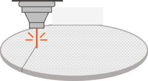
Wafer Dicing
Taking advantage of the non-thermal behavior of the ablation process with ultrafast lasers, chip manufacturers can selectively scribe low-k material and perform wafer dicing with limited heat-affected zone and delamination.
Probe Card Drilling
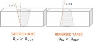
Thanks to their high peak power, ultrafast lasers are considered the Swiss army knife for material processing, allowing the drilling of soft polymers, hard ceramics, and metals. The lasers are used with 5-axis scanners to drill 0° taper holes with complex shapes in rigid probe card substrates at high speed.

Through Glass Via
Used in combination with chemicals, ultrafast lasers are the ideal tools to drill or etch holes in glass, accurate down to micrometer diameters, with a controlled taper over the full substrate thickness.
The introduction of GHz has also unlocked the possibility of drilling the substrate directly without requiring chemical etching, completely changing the manufacturing process.
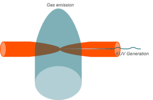
EUV Generation
Post-compression devices such our Compress, create pulses of only a few femtoseconds. Such peak power can be used for High Harmonics Generation, allowing the generation of a few nm / XUV wavelength beams.
EUV light is a powerful light source for Soft X-ray metrology, unveiling nanometer-scale patterns.
Thin Film Metrology
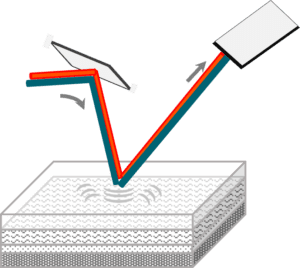
The picosecond acoustic technique is widely used for thickness metrology of thin films during the chip manufacturing process. It uses short pulses to pump and probe thin layer stacks in a non-destructive way, allowing see-through or opaque/metallic layers.