The power of 3D chip packaging
In the race towards chips always more powerful, embedded with more functionalities, and cheaper to produce, the past few years have seen the developments of 3D packaging designs.
By stacking and connecting different chips with different functions (for example Memory combined with IC), 3D packaging designs are reducing distances, and allowing more interconnections. This results in more efficient and faster systems.
To stake chips on top of the other, you need some separation layer. That layer acts as an isolator, to avoid any unwanted electrical connection or leakage between the chips. And a layer’s thermal expansion which will be in accordance with the thermal expansion of the chips, to avoid any tension/cracks created by the high heat released.
Silicon has been used as this separation layer, and a dedicated process called TSV (Through Silicon Via) has been put place.
Although, lately, Glass emerged as an alternative to Silicon, as its thermal and mechanical properties bring some advantages when combined with other material in a 3D stack.
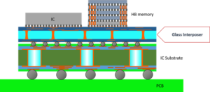
Figure 1 -Schematic of an Advanced Package, with a Glass Interposer linking insulated Chips to the substrate – Courtesy of Vitrion
Such Via or holes, have a high form factor, basically 1:10 if we take a standard 30um diameter via over a 300um thick glass wafer.
In order to create such Via, also called TGV (Through Glass Via), the most common method is the use a Laser Assisted Chemical Etching method. Using an ultrafast laser together with a Bessel beam (beam shaping such as provided by our GLASS module) one can create localized glass modification/microcracks, that will serve as a guide when then dipped into a chemical bath, resulting in etched Via.
This method works well but requires the use of chemical often harmful for the worker and the environment.
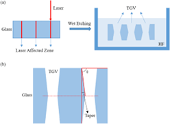
Figure 2 – Glass Module and principle of Laser assisted chemical etching process
But this may be soon overcome thanks to a new laser functionality developed by Amplitude, the GHz.
When replacing standard tens of MHz oscillators by GHz level internal repetition rate burst, light/matter interaction mechanism changes. When using the right amount of pulses, one can create a localized micro-welding effect, that helps removing the matter at a faster rate.
When combined with the proper focalization conditions, it can result in a confined ablation allowing really high aspect ratio via drilled at high speed, the 2 main contributors that allow people to start using it for TGV-like applications, while removing the need for the use of chemical.
After proof of concept in labs such as our partner CELIA, industrial players are now testing and fine tuning the laser parameters that would allow them to make it a industrial breakthrough.
The Satsuma X, with its several hundreds of uj, combined with our newly designed GHz front-end could be the tool of choice for this new field, and could see an adoption in the coming few months.
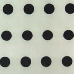
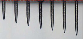
Figure 3 – SatsumaX and initial glass drilling results (courtesy of CELIA)
VIDEO >>